참고 기사 : www.graphenea.com/pages/what-are-graphene-field-effect-transistors-gfets
Graphene Transistors - GFET - Graphene Field Effect Transistors
What are GFETs? Simply put, graphene field-effect transistors take the typical FET device and insert a graphene channel tens of microns in size between the source and drain. Learn more about graphene transistors here. Graphenea is a leading graphene manufa
www.graphenea.com
위 기사를 참고하여 Graphene Field Effect Transistor의 활용성과 장점에 대해 정리해 보았다.
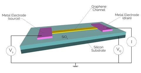
* Structure of GFETs
* GFET의 구조
Graphene field-effect transistors (GFETs) take the typical FET device and insert a graphene channel tens of microns in size between the source and drain. Being graphene, a lattice of carbon atoms that is only one atom thick, the channels in GFETs have unprecedented sensitivity, which can be exploited on a wide variety of applications such as photosensing, magnetic sensing and biosensing.
그래핀 FET는 일반적인 FET device의 소스와 드레인 사이에 수십 마이크론 크기의 그래핀 채널을 삽입한 것이다. 그래핀은 원자 하나의 두께를 가지고 있으므로, GFET의 그래핀 채널은 굉장한 민감성을 가지고 있는데, 광학 센싱, 자기 센싱, 바이오 센싱과 같은 여러 응용성을 가지고 있다.
When used in environmental sensors, this channel is typically exposed to permit binding and detection of receptor molecules such as glucose, cytochrome c, hemoglobin, cholesterol, or hydrogen peroxide onto the surface. When these molecules bind to the graphene channel, this alters the conductivity and overall device response. While the carbon in graphene typically does not react or bind with most materials, bioreceptors such as amino acids, antibodies or enzymes can be added through adsorption, or a linker molecule attached to the channel surface. Molecules can then attach to these sites through covalent bonding, electrostatic forces or Van der Waals forces, imparting an electronic transfer through the entire depth of the device.
환경센서로서 쓰일 때, 이 채널의 표면은 글루코스, cytochrom c, 헤모글로빈, 콜레스테롤, 과산화수소 같은 분자들의 결합과 감지를 위해 노출된다. 위와 같은 분자들이 그래핀 채널에 결합을 하게 되면, 디바이스의 전도성과 반응을 바꾸게 된다. 보통 그래핀의 탄소는 대부분의 물질과 반응이 없지만, 아미노산, 항체, 효소와 같은 바이오리셉터들은 흡수, 또는 링커 분자로서 연결될 수가 있다. 그 후 분자들은 공유결합, 전자기력, 반데르발스력과 같은 힘으로 연결될 수 있고, 디바이스의 전체 깊이까지 전자 전송을 남기게 된다.
* 그래핀 FET의 장점은?
- Unprecedented Sensitivity
- 전례없는 민감성
The two-dimensional structure of graphene has a number of benefits over bulk semiconductors, such as silicon, used in standard FETs. Because most semiconductor transistor sensors are three-dimensional, electric charge changes at the surface of channel do not always penetrate deeper into the device. This can dramatically limit the response sensitivity of the device. On the other hand, as the graphene in a GFET is only one carbon atom thick, the entire channel is now on the surface, which directly exposes the channel to any molecules present in the nearby environment.
This sensitivity was shown by scientists from the Manchester Centre for Mesoscience and Nanotechnology who proved that micrometer-sized sensors fabricated from graphene were capable of detecting individual gas molecules attaching to or detaching from the surface. As the addition or removal of a gas molecule causes a change of one electron within the graphene structure, small step-like changes in resistance can therefore be measured. Further research that demonstrates this heightened sensitivity includes the Department of Physics and Astronomy at the University of Pennsylvania which detected naltrexone (an opioid receptor antagonist) up to a limit of 10 pg per mL and the University of Plymouth’s Wolfson Nanomaterials and Devices Laboratory which used GFETs to detect the Human Chorionic Gonadotropin (hCG) antigen at concentrations of below 1 pg per mL.
그래핀의 이차원적 구조는 실리콘과 같은 두꺼운 반도체에 비해 여러 장점을 가지고 있다. 보통의 반도체 트랜지스터 센서들은 3차원 구조이기 때문에, 채널 표면의 전하 변화는 디바이스 깊숙히 전달되지 않는 경향이 있다. 이것은 디바이스의 민감도를 굉장히 떨어뜨리게 된다. 하지만 GFET의 그래핀은 원자 두께이므로, 표면 자체가 채널이고, 채널 전체가 주위 환경의 분자들에 노출되게 된다.
이 민감성은 Manchester Center for Mesocience and Nanotechnology의 과학자들로부터 증명되었는데, 마이크로미터 크기의 그래핀 센서가 하나의 기체 분자를 감지하는데 성공하였다. 하나의 기체 분자가 결합하고 떨어짐에 따라 계단식의 조그만 저항 변화들이 관측되었다.
... 뒷 얘기는 엄청 작은 농도에서 물질 detection이 가능했단 얘기...
- Fewer Molecular Defects
- 분자적 결함도가 낮다
Semiconductors such as silicon are ineffective when produced to be as atomically thin as graphene. This is because surface defects, or dangling bonds, tend to dominate at these thicknesses, which limits the overall sensitivity of the device. Such bonds form additional defects in the sensor’s semiconductor channel, and make non-specific binding possible, giving rise to false positives. This is unlike graphene which can be produced in a single layer with a high degree of accuracy and precision. Furthermore, a two-dimensional material such as graphene, produced efficiently, will have much less dangling surface bonds.
위의 본문은 실리콘 반도체가 그래핀 같이 원자 두께로 제작될 때에는 분자, 구조적 결함이 생긴다는 것을 설명한다. 표면 결함, 불완전 결합 등이 존재하게 되며, 민감성을 떨어뜨린다. 실로콘 반도체 채널의 결함 덕분에 false positive가 나오게 되는데, 그래핀은 높은 정확도와 완성도로 박막제조가 가능하므로 다르다.
- Superior Conductivity
- 뛰어난 전도성
GFETs also have a higher carrier mobility than traditional FETs, often reaching levels greater than 100,000 cm2V-1s-1 for hBN-encapsulated single-crystal CVD graphene. These devices also have a residual charge carrier density of the order of 5 x 1011 cm-2.
GFET는 전통적인 FET들보다 높은 carrier mobility를 가지고 있는데, hBN-encapsulated single-crystal CVD graphene의 경우 100,000 cm2V-1s-1와 같은 레벨에 도달할 수 있다. 또 5 x 1011 cm-2의 residual charge carrier density를 가지고 있다.